What is a PCB?
A PCB or Printed Circuit Board is an interconnect device that physically supports and electrically connects different components in an electronic circuit. PCBs are made by combining sheets of non-conductive material like fibreglass, composite epoxy etc. called as the substrate, coated with a layer of conductive material like copper or aluminium. Before the advent of PCBs, circuits were constructed through point-to-point wiring. These circuits experienced recurring failures due to loose contacts, ageing of wires and required intensive labour. PCBs on the other hand offer a sturdy base for the components to be mounted and the interconnections are made through immovable lines of copper called as "Traces". They are the go-to option for mass production and they've allowed electronic devices to be smaller & more compact. PCBs are used in most of the electronic devices manufactured today.
PCB - What is inside?
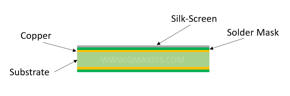
In its most basic form, the Printed Circuit Board or PCB, is made up of an insulating and non-conductive layer called the "Substrate" which is coated with a conductive layer of Copper. Copper is used as the conductive material in most cases given its high conductivity. The substrate may be coated with copper on either one or both sides. The solder mask, coated on top of the copper layer, prevents the formation of solder bridges between closely spaced solder pads. The solder mask is usually green in colour, though other colours like red, blue, black, etc., are also available. To identify components, test points and symbols on the board during assembly, a legend called the "Silkscreen" is printed on top of the solder mask. The silk screen is usually white in colour though black colour is used in case the Solder mask is of a lighter colour. This layer makes it easy for component placement through Surface-mounting Technology or Through-hole Technology.
Printed Circuit Boards (PCBs) are one of the most important parts of any electronic device. Each industry has its own specific requirements including different levels of operating temperature, vibration, corrosion resistance, current rating, electrical noise and heat dissipation. With years of experience in a wide variety of industries, our engineers have crafted this page putting together details from every aspect of PCB technology. These resources are your One Stop window to PCB fundamentals.
PCB Resources
PCB Types
PCB Technology
Design
Materials
Surface Finishes
Plating
PCB Terminology
PCB Types
PCBs are designed to suit different needs and purposes. They are predominantly classified based on the number of copper layers and can be further classified depending on the type of substrate used.
Single-sided PCB
Single-sided PCBs, also known as single layer PCBs, are the simplest type of PCBs. Made up of a single layer of base material, they are coated on only one side with a layer of conducting material. The solder mask is applied to the copper followed by the silk screen. Single layer PCBs are easy to design and manufacture, making them the ideal choice for low cost and bulk manufacturing applications.
Double-sided PCB
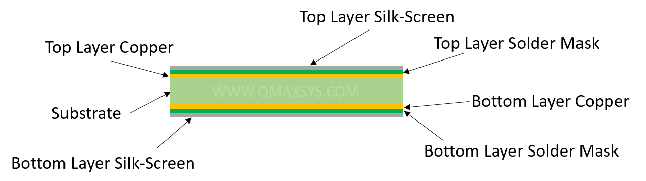
The double-sided PCBs or the double-layer PCBs have conducting material on both sides of the base material. This allows components to be placed on both sides of the board using Through Hole or Surface Mount Technology. Double sided PCBs have more surface area facilitating placement of more components.
Multi-layer PCB
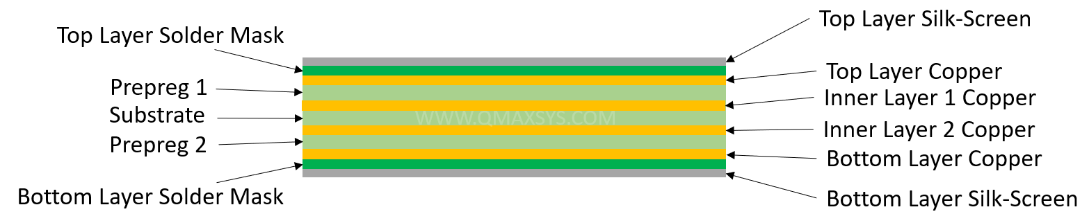
The multi-layer PCB can have 3 to multiple layers of conducting material (copper sheets) with insulating "prepreg" layers in between. Prepregs keep the inner core material attached to the copper, so they can be bonded into a single structure using heat and pressure. A typical 4 layer PCB will be stacked like this:
Bottom copper foil - Prepreg sheets - Inner core layer - Prepreg sheets - Top copper foil
Complex PCBs used in defence, aerospace, avionics and telecommunication applications can have over 50 layers.
HDI PCB (High Density Interconnect)
An HDI PCB has a higher wiring density per unit area compared to a typical PCB. They contain blind, buried vias and micro vias up to .006" or less in diameter. The high wiring density of the board helps to increase the number of electrical connections and reduce the size and weight of a device.
Metal Back PCB
Metal backed PCBs have metal substrates instead of FR4 or other non-conducting materials. There is a layer of ceramic insulation between the Metal Substrate and Copper Traces. These are used where higher levels of heat dissipation is required. Metals like aluminum, copper or brass with a thickness of 0.4mm to 10mm are used as substrates. Most importantly, these boards are cost-effective, light-weight, strong and durable, making them ideal for any application. The cooling properties of the metal-backed boards allow the device to be driven harder.
Single-sided Flex PCB
A single-sided flex PCB consists of a flexible polyimide film for the substrate, a copper sheet to etch the circuit pattern, a bonding adhesive, and a polyimide coverlay for insulation. The Flexible PCBs or Flex PCBs cost more to design and manufacture than other PCBs. In larger devices rigid PCBs are used, and when the device is compact (camera, mobile phone, etc.), the PCB must be flexible enough to fold and fit into the device, requiring a flex PCB. Flex PCBs can replace rigid PCBs by conforming to any shape.
Double-sided Flex PCB
A double-sided flex circuit has two conductive layers, one on each side of the substrate. In these boards, the traces are accessible from both the top and bottom, and the layers are connected through ‘plated through-holes’ (PTH). Double-sided flex PCBs can be used in ground & power plane applications, shielding applications or dense surface-mount assembly.
Multi-layer Flex PCB
In multi-layer flexible circuits, there are three or more conductive layers interconnected with ‘plated-through holes’ (PTH). Each layer consists of a flexible polyimide film for the substrate, a copper sheet to etch the circuit pattern, a bonding adhesive. These layers are stacked in sequence, with a polyimide coverlay for insulation in between them, to create a multi-layer flexible PCB. Multi-layer flex circuits can have up to 8 conductive layers.
Semi-Flex PCBs
Semi-flexible circuits are different from flexible circuits. They are made from a portion of rigid FR-4 PCBs, where they undergo ‘thinning’ to make the board bendable. Since they are made from FR-4 material, semi-flex PCBs are a cheaper alternative to Rigid-Flex circuits. The flexibility feature of this rigid PCB simplifies handling during assembly and installation.
Rigid-Flex
Rigid-flex PCBs are a combination of rigid and flexible PCBs. Layers of flex PCBs combined with one or more rigid PCBs are called rigid-flex boards. Rigid-flex PCBs have a lower part count since the wiring is combined into a single board, making them the optimal choice for compact and small devices. They are small, weight and thickness.
PCB Technology
There are two main technologies used for mounting components on PCBs. One is "Through-hole technology" and the other is "Surface-mount technology".
Surface-mounted technology (SMT)
In Surface-Mount technology, Components are soldered directly onto the board without drilling any holes. This method allows more components to be placed resulting in a smaller and lighter PCB. Surface mount technology is cost-effective, more efficient and much faster than Through-hole technology. Most of the industries today prefer SMT for these reasons.
Through-hole technology (THT)
In the Through-Hole method, where components with leads are inserted into holes drilled in the PCB. The leads are then soldered onto the copper pads. THT offers unique benefits like stronger bonding than SMT, easier component removal for testing etc. Before the invention of surface Mount Technology in the 80s, THT was the only technology used for the assembly process. Components used in THT are larger than the ones used in SMT PCBs and hence are mostly suitable for low density applications. This has lead to the decrease in usage of THT technology over the years.
Design
Blind and Buried Vias
Vias are the copper-plated holes that allow the layers of the board to connect to each other. A blind via is a hole that connects the outer layer to the inner layers. The hole isn’t drilled completely through the board, but up to a certain layer inside the board making the outer layer and inner layer interconnected. A buried via is a hole drilled to connect one or more inner layers, they are not visible from the outside.
Microvia
Microvia are minute holes drilled into the board using laser technology to create electrical connections between the layers in High Density Interconnect (HDI) PCBs. These microvia can be as small as 150 micrometres in diameter. The holes are plated with copper as in case of a regular VIA.
Via-in-Pad
When the via is placed in a copper pad, it is called a ‘Via-in-pad’. Via-in-pad allows the use of smaller components, reducing the size of the PCB. The via can be filled with conductive or non-conductive filling for soldering.
Materials
PCB materials are of immense importance because they provide insulation between copper layers, determine the performance of the board and suitability for an application. These materials are classified based on their properties.
CEM-1
CEM-1 is a composite material made of woven glass fabric and cellulose paper, combined with epoxy resin. This material is used in single-sided PCBs for simple applications. It has high flexural strength, higher transition temperature than FR-4 as well as good mechanical and electrical properties.
CEM-3
CEM-3 is developed based on FR-4. This material is milky-white in colour and mostly used in the manufacturing of double-layered and multi-layered PCBs. CEM-3 is a cheaper replacement for FR-4 in the Asian market with production, application and growth rate higher than FR-4.
Surface Finishes
Surface finish is the coating done on the copper pads. It is done to ensure the solderability of the board and to prevent oxidation and deterioration of the copper.
ENIG (Electro-less Nickel Immersion Gold)
ENIG is a double-layer metallic coating, where the copper surface is coated with nickel and a thin layer of immersion gold above that to prevent oxidation. It is lead-free, has a longer shelf-life and can be used on critical surfaces making it one of the most popular finishes.
HASL (Hot air solder levelling)
HASL is one of the most common surface finishes used in the industry. The PCB is immersed into molten tin/lead alloy after the solder mask is applied. The copper surface is covered with molten solder and the excess is removed by passing the PCB through hot-air knives. This process removes the unwanted solder by blowing hot air over the board.
Lead-free HASL
In lead-free HASL, a solder material like Tin-copper is used instead of lead. The Tin-Nickel solder is molten, and the board is immersed into it. Lead is toxic and harmful, which makes lead-free HASL preferred by most industries.
OSP (Organic Surface Protection)
It is an organic surface finish to prevent oxidation of copper. OSP is a water-based finish made from organic preservatives to protect copper until assembly with a shelf life around 9 months given its organic structure. This coating is applied to the copper surface through a conveyorized process where the finish selectively bonds to the copper surface. It is non-toxic and completely environment-friendly when compared with other surface finishes. OSP is re-workable, cost-effective and maintains planarity.
Immersion Silver
Immersion silver is a method of coating the exposed copper pads on the PCB with silver and OSP. The OSP prevents tarnishing of silver, extending the shelf life up to a year. The silver coating is preferred because it gives a flat coating making it easy to solder. Immersion silver is a very simple process suitable for fine traces.
Immersion Tin
The copper pads in the PCB are coated with a layer of tin. The immersion tin forms a copper-tin inter-metallic joint. This coating provides a 6-month shelf-life to the board and gives a dense, uniform coating which makes it suitable for Surface mounting technology. Immersion tin is sometimes used as an alternative to lead-based surface finish for its sustainability.
ENEPIG (Electroless Nickel Electroless Palladium Immersion Gold)
Nickel is deposited over copper pads using electroless deposition method. It is then turn coated with layer of palladium. Palladium covers the nickel and prevents it from blackening. Palladium is coated with immersion gold providing good solder joint and gold wire bonding reliability. ENEPIG gives a shelf life for more than a year and is suitable for a wide range of assembly requirements.
Hard Gold
Hard Gold is a layer of gold alloy with added metals to harden it for increased durability. An electrolytic process is used to apply this surface finish and is commonly applied to areas that should withstand repeated use. Hard Gold is suitable for contact switch, gold wire binding as well as conducting electric tests. It has a shelf life of up to 12 months.
Soft Bondable Gold
Soft gold is the purest form of gold without any additional elements. The gold coating is 99.9% pure with a knoop hardness range of 60-85. An electrolytic process is followed to apply the soft gold finish. The finish is suitable for wire bonding operations as it produces a stronger joint.
Plating
Plating is the process of depositing metal (copper) on the PCB surface through an electrochemical process.
Edge Plating
Conductive material coated around the external edges of a PCB, covering all the layers, is called edge plating. Edge plating is used to connect copper traces or planes in between layers of the same board and these boards are used in applications like connectors that slide into metal casings. This type of plating is a solution to electromagnetic emissions radiating out of the edges of a backplane.
Castellations
Castellations are plated through holes that are located at the edge of printed circuit boards. They are half holes that are intended to create links between a module and a board or between two boards. There are different designs for castellated mounting holes such as half holes, holes with smaller half holes, and holes tangent to the board’s edge.